INTEL SCALABLE PERFORMANCE PROCESSORS
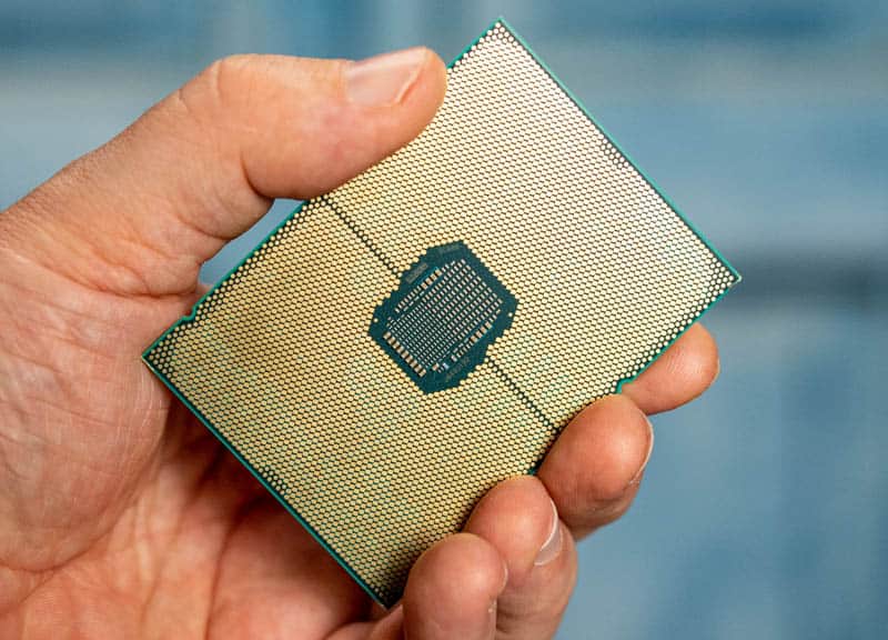
Intel’s Xeon Scalable Performance family of processors are built on a mature platform that enables high performance and efficiency in demanding server applications such as AI machine learning and cloud computing. We’ll be going over the first 3 generations of the Intel SP platforms below, comparing the generational improvements made with each revision.

First generation Xeon SP systems are based on the Skylake-SP microarchitecture, which is a high-performance modern architecture built on the 14nm manufacturing process. Skylake-SP boards have support for up 8 socket configurations in the Xeon Platinum grade, 4 sockets in Xeon Gold, and 2 sockets in Xeon Silver and Bronze based systems. SKUs with the M designation can operate up to 1536 GB of memory per socket; this number is limited to 768GB of memory otherwise. All SKUs support up to 12 DIMMs of DDR4 memory per socket with memory clocks up to 2666MHz. The SKUs featuring the F designation feature integrated OmniPath fabric interconnect communications between processors while the SKUs featuring the T designation are optimized to perform at higher thermal-cases and provide extended reliability. Intel’s OmniPath technology allows for low-latency, high-bandwidth communications between processors for highly scalable applications that benefit from improved socket-to-socket interaction such as with machine learning. In addition, Xeon Platinum and most Xeon Gold SKUs have two dedicated FMA units per core for handling AVX-512 instructions, the rest having one FMA unit per core. Core counts range from as little as 4 cores up to 28 cores with HyperThreading (58 virtual cores total) and processor clocks from 1.7GHz up to 3.6GHz (3.8 via single-core boost over short periods). All this results in a highly scalable platform that provides plenty of computing power and can be built to meet both budgetary and performance requirements of the end user.
Second Generation Xeon SP systems are based on the Cascade Lake-SP microarchitecture, which is an optimized revision of the Skylake-SP microarchitecture used in the prior generation. This means that while it retains the 14nm manufacturing process of the previous generation, improvements have been made to increase efficiency and performance across the board. This was also the first-generation of Xeon SP to introduce support for 3D XPoint non-volatile memory modules (also known as Optane), built-in protections for the infamous Meltdown and Spectre exploits as well as the Deep Learning Boost instruction set for machine learning applications. A majority of the features and benefits found in the first generation Xeon SP product line is carried over to the second generation. However, thanks to improvements in optimization, processors are now capable of higher boost clock rates (up to 4.5Ghz) for increased short-term performance as well as lower TDP or higher clock rates when compared to equivalent 1st generation SKUs during typical operation. The platform has also been improved to support up to 2933MHz memory speeds with capacity increased to 1TB per socket on non-M SKUs and 2TB per socket on M SKUs, plus a new L SKU that supports up to 4.5TB of memory per socket. To put simply, the second generation provides improved performance across the board over the first generation with the biggest gains made in machine learning applications, memory capacity and performance, short-term single-core performance, and overall security.

Third Generation Xeon SP systems are split into two different microarchitectures: Cooper Lake-SP for 4-8 socket applications and Ice Lake-SP for single and dual socket applications. Cooper Lake-SP is built on the 14nm process much like its predecessors while Ice Lake-SP is the first Scalable Performance platform to take advantage of the new 10nm manufacturing process from Intel. Cooper Lake is yet another optimization on the venerable Skylake microarchitecture and provides many of the same performance benefits of the 2nd generation 4 -8 socket models while adding support for faster memory (up to 3200MHz DDR4), support for 2nd generation Optane memory, and a doubling of the UPI links. Additionally, Cooper Lake adds the new bfloat16 instruction set to the Deep Learning Boost series of machine learning optimized instruction sets. Typical processor clock speeds have also been improved across the board thanks to further optimizations to the microarchitecture. Where things get exciting in the third generation of Xeon SP products are the Ice Lake-SP based components. Thanks to the die shrink, Intel is able to provide higher levels of per-processor performance with increased core counts (up to 40 cores per socket or 80 virtual cores via HyperThreading). As with most die shrinks, nominal TDP per core has also been improved, allowing for higher typical clock speeds and/or lower average operating TDPs. Memory support largely mirrors it’s Cooper Lake-SP brethren but also includes support for high speed LPDDR4X memory running at 3733MHz. Instructions-per-clock improvements and an increased L3 cache capacity allows for higher performance across the board as well. Overall, the 3rd generation of Xeon SP systems will provide a noticeable improvement in raw performance over the previous generation, especially in highly parallel workloads and applications that can take advantage of the higher core count/density of the Ice Lake-SP platform.
